|
|
|
| Objective | Overview | R&D Subjects |
|
 |
Project Manager: Kazutoshi Kobayashi | ||
| Professor, Director, |
Dept. of Electronics, Graduate School of Science and Technology, Kyoto
Institute of Technology Kyoto Semiconductor Co-creation Lab., Kyoto Institute of Technology |
||
| |
|||
| ・ | Long-Term Stable Operation of Qubit Control Device has been Demonstrated The research and development group managed by PI Takefumi Miyoshi of this project Qubecs) has developed "QuEL-1 SE," a qubit control device that achieves long-term stabilization of microwave signals used to control superconducting qubits. The performance has been experimentally demonstrated. For details, please see the press releases as followings. https://qiqb.osaka-u.ac.jp/newstopics/pr20260327 https://prtimes.jp/main/html/rd/p/000000003.000173953.html |
|
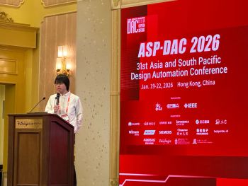
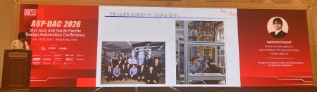
| ・ | Takefumi Miyoshi (QuEL, Inc.), PI had a Key Note speech at 31st Asia and South Pacific Design Automation Conference (APC-DAC 2026)
. Keynote VI : Thursday, January 22, 09:05-09:50 "Design and Implementation of Control System for Quantum Computers" |
 |
 |
||
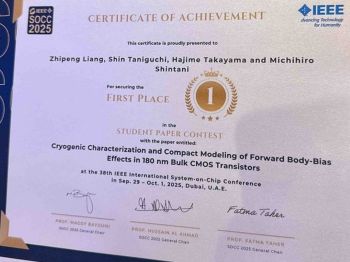
| ・ | Zhipeng Liang, a Master's course student in the Shintani Laboratory at
Kyoto Institute of Technology, has recieved "First Place" from
IEEE SOCC 2025 Student Paper Contest. "Cryogenic Characterization and Compact Modeling of Forwad Body-Bias Effects in 180 nm Bulk CMOS Transistors", Zhipeng Liang, Shin Taniguhi, Hajime Takayama and Michihiro Shintani |
 |
| ・ | Open Campus 2025, Kyoto Institute of Technology was held on August 8th through 9th. VLSI Systems lab., Kyoto Institute of Technology held an open laboratory tour, and held an exhibition and explanation of a quantum computer control devices from QuEL Inc., which is a principal investigator in this project (QUBECS). For pictures of the open campus, click here |
|
| ・ | Professor Kazutoshi Kobayashi is introduced as one of only three university professors in Japan who
teaches semiconductor integrated circuit design. Yahoo News: "If we want to revive Japanese semiconductors industry, we need at least 100 billion yen in support for semiconductor integrated circuit design." August 1, 2025 https://news.yahoo.co.jp/expert/articles/ec907151e92e7538beeb2df1530333ba2d1ec211 |
|
| ・ | Part of the results of this project (QUBECS) have been published as a "100% domestic quantum computer". https://www.youtube.com/watch?v=dy_eBN4iSCs July 29, 2025 |
|
| ・ | "100% domestic quantum computer has been operated on July 28th!" A new "Quantum Experience" is offered to Expo visitors by connecting to cloud from the Expo site (July 28, 2025) Moonshot Goal 6 "Development of Scalable Highly Integrated Quantum Bit Error Correction System: QUBECS" (Project Manager: Kazutoshi Kobayashi) is supporting the 1st domestic quantum computer, and the advanced control device developed by QuEL, Inc. collaborating in this project QUBECS, is used. *Press release issued by Center for Quantum Information and Quantum Biology (QIQB), The University of Osaka on July 28. https://qiqb.osaka-u.ac.jp/newstopics/pr20250728 |
|
| ・ | On May 19, 2025, Nikkei XTECH pressed the activities of QL Co., Ltd., who
is a member of this project that develops and sells quantum computer control
and relay devices. https://xtech.nikkei.com/atcl/nxt/mag/ne/18/00001/00523/ |
|
| ・ | Graduate school student, Zhipeng Liang (M1) of PI Shintani's lab. presented
his research results and won the Excellent Poster Award at the System and
LSI Workshop 2025 held at the University of Tokyo's VDEC on May 13~14th,
2025. https://pdf.gakkai-web.net/ieice/icd/doc/poster_program_2025v3.pdf |
|
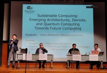
| ・ | PM Kobayashi spoke on the stage as a panelist in the panel discussion "Sustainable
AI: Emerging Architectures, Devices, and Quantum Computing Towards Future
Computing" at COOL Chips 28, held on April 17, 2025 Slide is here |
 |
| ・ | QuEL, Inc., which is partly responsible for this project, has developed
a control device which will hold the fate of quantum computers. (Published
on March 24, 2025) Detail |
|
| ・ | IEICE General Conference, Organized session, "Trends in Quantum Computing:
From Circuits and Devices to Applications" (held at March 26, 2025),
IEICE Public Site |
|
| ・ | Socionext Inc. has signed a strategic partnership with Google Quantum AI
to develop quantum control chips. Press by Nikkei XTECH (February 27, 2025) * This announce is not related to our project MS6 Qubecs. |
|
| ・ | PM K. Kobayashi a lecture at the 3rd symposium FY2024 of Kansai Chapter
of Cryogenics and Superconductivity Society of Japan held at February 5,
2025. Kansai Chapter Information site |
|
| ・ | The 11th Workshop of JSAP Industry and Academy Collaboration Committee
on Ultimately Integrated Electronics, chaired by PM K. Kobayashi, was held
with a thema, "The Frontline of Quantum Computers" at January
20, 2025. The 11th Workshop site |
|
| ・ | Associate Professor, A. Tsuchiya of The University of Shiga Prefecture
had a lecture entitled "Leading-edge research and the future of integrated
circuit design" to introduce "Integrated Circuit Research"
to university and technical college students at a Symposium of "Green-niX",
Toyohashi University of Technology. (Sept. 26, 2024) TUT IRES2 site |
|
| ・ | Project Manager, K. Kobayashi had a Keynote Speech in Quest-2024 (Sept. 9, 2024) The slides are listed in the"Pablication List" as below. |
|
| ・ | Site visit 2024 (July 30, 2024) |
|
| ・ | KIT and Kioxia Corporation have entered into a cross-appointment agreement
with the aim of promoting research and development on design technology
for semiconductor integrated circuits (LSIs) that operate in cryogenic
environments, and human resources development in the semiconductor industry.
(KIT Press relese is May 17, 2024) |
|
| ・ | Nature: Nature Focal Point on Quantum computing in Japan (Top page of the feature) "Quantum computers shoot for the moon" (Our project: QUBECS) |
|
| ・ | Introduction movie of our project on APS TV March meeting 2024 |
|
| ・ | Moonshot International Symposium for Goal 6 held at April 23, 2021 (Public video site) |
|
| * Publications List for The 1st Generation Project (~March 2026) * Publications List for The 2nd Generation Project (April 2026~) |
| Objective |
| This research and development project aims to realize an agile error
correction system for a wide variety of qubits, superconducting qubits,
neutral atoms, and so on, and to realize a small and low-power qubit controller
for superconducting qubits. The Moonshot Goal 6 by 2050 will target the
realization of a large-scale and fault-tolerant general-purpose quantum
computer. In this research and development project, we will realize an
error correction system and a qubit controller that can handle up to 1
million qubits by combining a communication network between upper-level
medium-sized qubits and top-level qubit hardware. |
 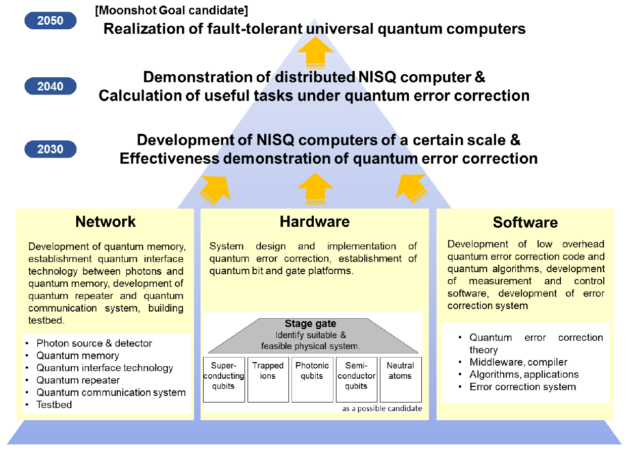 |
| R&D Subjects |
|
| Research and development theme 1: Hardware algorithms and proof-of-concept systems for quantum error correction |
|
 |
Principal Investigator: Kentaro Sano (RIKEN) Overview: Development of hardware algorithms for quantum error correction and build demonstration systems using FPGA boards and FPGA clusters optimized for online quantum error correction to realize a scalable backend system for error correction. In addition, we will conduct simulated error correction experiments for superconducting qubits and demonstration experiments for error correction for neutral atom qubits, respectively. |
| Development Goal: To actually build a demonstration system using FPGA boards and FPGA clusters optimized for online quantum error correction, and implement the hardware algorithm for quantum error correction. In addition, we will collaborate with the Yamamoto Project and the Omori Project within MS to conduct simulated error correction experiments for superconducting qubits and demonstration experiments for error correction for neutral atom qubits, respectively. |
|
| Research and development theme 2: Quantitative evaluation of the FTQC architecture |
|
 |
Principal Investigator: Junichiro Kadomoto (The University of Tokyo) Overview: For realization of large-scale quantum computers, we will formulate quantum computer architectures targeting superconducting qubits, optical qubits, and distributed configurations. We will optimize the overall design, including error correction codes and logic operations, by implementing key components as ASICs, and establish design guidelines that combine implementability and scalability through quantitative evaluation based on indicators such as the number of physical qubits, power consumption, and latency. |
| Development Goal: To quantitatively evaluate the optimized architecture through ASIC implementation and conduct architectural design and optimization studies for the overall architecture of a superconducting quantum computer, including generalized lattice surgery, assuming ASIC implementation. |
|
| Research and development theme 3: Scalable error correction system integration technology | |
 |
Principal Investigator: Yasunori Osana (Kumamoto University) Overview: Realization a high-throughput, low-latency, reliable, and scalable interconnection network by interconnecting numerous FPGAs that constitute a quantum front-end controlling qubits and a back-end performing quantum error correction, integrating the entire system as a single entity. Furthermore, it investigates reliability-related issues such as software errors in FPGAs that become problematic when scaling up the back-end, and identifies the necessary countermeasures for realizing a quantum error correction back-end on the scale of 1 million qubits. |
| Development Goal: To develop an interconnection network to connect numerous FPGA nodes that make up the front-end and back-end. We will combine a dedicated protocol with Ethernet to achieve an optimal and scalable integrated interconnection network tailored to the bandwidth and latency requirements at various points in the system. Furthermore, we will establish soft error countermeasures necessary for systems operating numerous FPGAs constructed with advanced micro-processes, define a low-latency, high-reliability connection method between the front-end and back-end, and measure and evaluate bandwidth, latency, and reliability. |
|
| Research and development theme 4: FTQC Abstraction Layer Compiler | |
 |
Principal Investigator: Toru Kawakubo (QunaSys Inc.) Overview: Development of a compiler and runtime processing system necessary to execute arbitrary logic quantum circuits, including Clifford and non-Clifford operations, on superconducting qubits. And to connect and integrate with qubit control devices and decoders, and demonstrate the execution of logic quantum circuits in conjunction with other projects within the same categor. |
| Development Goal: To develop a compiler and runtime processing system necessary to execute arbitrary logic quantum circuits, including Clifford and non-Clifford operations, on superconducting qubits. In conjunction with other projects within the same project, we will connect and integrate these systems with qubit control devices and decoders to demonstrate the execution of logic quantum circuits. |
|
| Research and development theme 5: Applications of design automation technology for quantum computers | |
 |
Principal Investigator: Kazutoshi Wakabayashi (The university of Tokyo) Overview: To comprehensively handles core compiler operations such as scheduling lattice surgeries, arranging logical qubits (Placement, Mapping), and optimizing the supporting physical resources. |
| Development Goal: To develop a scheduling algorithm for lattice surgery used in fault-tolerant quantum computers and implement it in a compiler for quantum computers. This will ensure that the compiler functions correctly, performs appropriate scheduling, and issues instructions correctly. |
|
| Research and development theme 6: Implementation of coding methods other than surface coding on multi-FPGA | |
 |
Principal Investigator: Hideharu Amano (The University of Tokyo) Overview: We will explore the possibilities of FPGA systems that perform online error correction using encoding methods other than surface codes, such as the recently popular qLDPC codes and color codes. And also explore the suitability of these systems not only for superconducting quantum computers, but also for neutral atom and ion trap type quantum computers. |
| Development Goal: To performed real-time coding on the actual system, compared with surface coding, and coding methods other than surface coding are implemented on a multi-FPGA. |
|
|
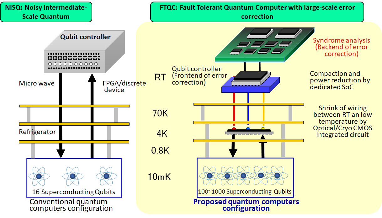
| Research and development theme 1: Radicalization of advanced controllers (front-end) |
||
 |
Principal Investigator: Takefumi Miyoshi (QuEL, Inc.) Overview: Realization of Fault-Tolerant Quantum Computing (FTQC) requires a control device capable of controlling a large number of qubits with high stability and reliability. This research aims to clarify the architecture and implementation method of a control device that possesses the stability and scalability necessary for qubit control assuming FTQC in 2030, and to present design guidelines for an integrated system for FTQC that works in conjunction with an error correction backend. |
|
| Development Goal: - Construction of a quantum computing system using physical qubits for FTQC - Realization of a front-end for hundreds to thousands of qubits for FTQC - Realization of a high-density signal generation front-end for semiconductor quantum dot control - Realization of a control front-end for ion traps using signal multiplexing - Realization of a front-end system for demonstration experiments using Cryo CMOS A front-end system compatible with various qubits controls the physical qubits. |
||
|
| Research and development theme 1: Design Technology for Low-Temperature Optical Integrated Circuits for Scalable
Classical-Quantum Interfaces |
||
 |
Principal Investigator: Jun Shiomi (Osaka University) Overview: Operating optical integrated circuits in cryogenic environments is a promising solution for reducing the number of wiring cables between ambient and cryogenic temperatures and ensuring the scalability of physical qubits. This project explores design techniques for optical integrated circuit elements in low-temperature environments. Specifically, it studies optical interfaces for classical-quantum interfaces that realize low-power and high-speed information communication and processing, and builds the foundation for a design environment for scalable error correction systems in line with this objective. |
|
| Development Goal: To design an optical integrated circuit for controlling superconducting qubits and verify the connection and operation of the superconducting qubit control circuit and the optical interface. |
||
| Research and development theme 2: Optical interface between room temperature and 4K |
||
 |
Principal Investigator: Hidehisa Shiomi (Osaka University) Overview: In control architectures, the introduction of optical interfaces is promising as a means of transmitting large-capacity digital signals exchanged between room temperature systems and low-temperature systems within refrigerators with low thermal load and broad bandwidth. Optical fibers possess both ultra-broad bandwidth and low thermal conductivity, making them a promising candidate for control wiring in future large-scale quantum computers. Previously, analog signal transmission based on Radio over Fiber has been proposed as a microwave optical transmission technology between room temperature and low temperature, but the heat generated by photoelectric conversion has been a major challenge. This project aims to reduce heat generated by photoelectric conversion and improve transmission efficiency by assuming digital optical transmission instead of analog transmission. |
|
| Development Goal: 1. Constructed a 16-channel optical transmission path evaluation
system to evaluate the feasibility of high-capacity optical transmission.
2. Systematically organized design guidelines for fiber chip-to-fiber connection
structures with low-temperature implementation in mind. 3. Conducted an
integrated evaluation as a signal processing system assuming a room-temperature-low-temperature
optical interface, and organized design guidelines for the application
of qubit control. The room-temperature-low-temperature optical interface reduces the number of wires and heat inflow. |
||
| Research and development theme 3: Scalable photoelectric hybrid qubit control architecture | ||
 |
Principal Investigator: Ryosuke Matsuo (The University of Tokyo) Overview: This project aims to overcome scalability challenges by installing a photoelectric integrated control system in a cryogenic environment and controlling qubits. However, cryogenic environments impose very strict constraints on the power consumption and circuit area of control circuits. By utilizing the properties of photoelectric integrated circuits, we will explore a unique architecture that can reduce communication costs with room temperature and the cost of circuits installed in cryogenic environments. |
|
| Development Goal: To develop architecture optimization methods and to elucidate a qubit control
architecture that can be implemented in cryogenic environments. |
||
| Research and development theme 4: Scalable mixed-signal system for photoelectric IF | ||
 |
Principal Investigator: Hiroki Ishiguro (Keio University) Development Goal: We will develop a mixed-signal integrated circuit for optoelectronic integration that connects optical integrated circuits and cryo CMOS integrated circuits at room temperature and cryogenic temperatures. By introducing mixed-signal technology into circuits that convert the ultrafast data transmission rate of the optical interface to the operating speed of the cryo CMOS integrated circuit, and power supply circuits that suppress power supply losses due to power cables with high wiring resistance in the refrigerator, we will design and prototype circuits for optoelectronic integration with high power efficiency and build a foundation for a scalable classical-quantum interface. |
|
| Development Goal: To demonstrate the operation of the photoelectric integrated IF at cryogenic temperatures, and evaluate the achievement of the objective and the criteria for judgment: Confirm the operation of the photoelectric integrated IF at cryogenic temperatures. | ||
| Research and development theme 5: Development of transistor modeling technology for scalable cryogenic integrated
circuit design. |
||
 |
Principal Investigator: Michihiro Shintani (Kyoto Institute of Technology) Overview: Cryo CMOS technology, which operates silicon CMOS circuits controlling qubits at cryogenic temperatures, is a promising solution for reducing the number of connections between room temperature and cryogenic temperatures and ensuring the scalability of physical qubits. On the other hand, establishing a highly accurate transistor model in cryogenic environments is essential for realizing large-scale integrated circuits with Cryo CMOS technology. In this project, we will elucidate the physical behavior of silicon CMOS at cryogenic temperatures and reflect it in the model, as well as develop a Process Design Kit (PDK) environment that enables large-scale integrated circuit design even under the strict power constraints of a 4K environment. |
|
| Development Goal: 1. Release of a transistor model that takes into account characteristic
variations and self-heating. 2. Release of an improved version of the transistor model. Evaluation and judgment criteria for achieving the objective: Actual circuit operation is simulated using a commercially available SPICE simulator. |
||
| Research and development theme 6: Construction of a Cryo CMOS integrated circuit design platform | ||
 |
Principal Investigator: Takashi Sato (Kyoto University) Overview: For integrated circuits for scalable classical-quantum interfaces, collaborative optimization across multiple layers, including devices, circuits, architectures, and applications, is necessary, and design automation technology is a common foundational technology. Currently, there is a lack of established techniques for predicting performance indicators such as power consumption and processing speed early in the design process, which are particularly important when developing systems for controlling quantum devices in cryogenic environments or intermediate temperature environments between room temperature and cryogenic conditions, as well as design methodologies for optimizing circuit design based on these predictions. Furthermore, reliability is essential to enable long-term and stable control of a large number of qubits. This research project aims to develop design and optimization methods for scalable cryogenic integrated circuits that enable performance prediction at various ambient temperatures. |
|
| Development Goal: By establishing an optimization flow for cryogenic environments and designing according to this optimization flow, to predict the circuit performance of design results assuming extremely low temperatures, and to demonstrate the maximum performance. performance. |
||
| Research and development theme 7: PDK development for Cryo CMOS devices and wiring elements | ||
 |
Principal Investigator: Ken Uchida (The University of Tokyo) Overview: To develop a PDK for Cryo CMOS primarily targeting the 80–3 K range, by developing device and wiring models based on the physics of carrier and thermal transport. In the first year, a high-vacuum multi-layer deposition system will be set up, and alloy nanofilm temperature sensors operating down to the 3 K range will be fabricated. Low-temperature thermal conductivity of semiconductor-related materials will be obtained using the 3ω method. Based on the obtained thermal property data, wiring resistance models considering self-heating and electrical property models of devices such as MOS capacitors and pn junctions at cryogenic temperatures will be developed. Furthermore, in collaboration with the Tarucha Group, the project aims to extend to the 10 mK range and establish a low-temperature PDK foundation highly compatible with quantum integrated circuits. |
|
| Development Goal: 1. Release of Cryo CMOS Material Thermal Data Set v1.0 (PDK attachment). 2. Release of Thermal-aware Cryo Interconnect PDK v1.0 (80–3 K) board. 3. Release of PDK (ver.1) boards for MOS capacitors, pn junctions, and MOS transistors. These releases enable the implementation of PDKs compatible with mK/4K. |
||
|
| Research and development theme 1: Digital circuit technology for front-end and back-end applications |
|
 |
Principal Investigator: Kazutoshi Kobayashi (Kyoto Institute of Technology) Overview: To design the digital section of an SoC for superconducting qubit control that operates in a cryo environment, and in collaboration with PI Kadomoto and PI Wakabayashi (item 1), we will design a low-power error correction circuit, run it on an FPGA, and consider ASIC implementation. In conjunction with the Takahashi project, we will examine the specifications of an SoC that operates in a cryo environment for ion trap qubit control, and use external contractors to create an LSI. |
| Development Goal: 1. Re-conduct control experiments from a cryo environment. 2. Error correction experiments using a standalone FPGA and an error correction LSI. 3. Implementation of dynamic voltage control necessary for CCD operation. Perform ASIC implementation of the digital section and verify its operation. Gain insights into reliability in cryogenic environments. |
|
| Research and development theme 2: Development of RF front-end circuit technology to achieve scalability |
|
 |
Principal Investigator: Akira Tsuchiya (The University of Shiga Prefecture) Overview: Achieving scalability requires miniaturization, low power consumption, tolerance to environmental fluctuations such as temperature and voltage, and resistance to interference from other circuits. Simply converting existing systems to ASICs is insufficient. We will also perform optimizations, including architectural considerations to achieve a scalable RF front-end,. |
| Development Goal: To propose and demonstrate an RF front-end architecture that achieves scalability, and design and perform field evaluations of RF front-end circuits (TEGs) that have the potential to be scalable in the future. |
|
| Research and development theme 3: Automated design of DAC for qubit control |
|
 |
Principal Investigator: Nobukazu Takai (Kyoto Institute of Technology) Overview: Development of a digital-to-analog converter (DAC) that achieves low power consumption and high-speed operation. We will incorporate machine learning-based automated design into the DAC's elemental circuit design, significantly reducing design time. Using a 22nm CMOS bulk process, we will prototype the automated-designed DAC and evaluate it through measurement. The DAC and other group circuits will be configured as a qubit control circuit using chiplets to control the qubits. |
| Development Goal: 1. Control of qubits using a control circuit including a 1mW DAC. 2. Automatic design and synthesis of DAC circuits achieving low power consumption and high-speed operation, and review and addition of training data. To design and evaluate scalable DACs using automated design methods. |
|
| Research and development theme 4: High-speed ADC for front-end | |
 |
Principal Investigator: Masaya Miyahara (High Energy Accelerator Research Organization) Overview: Development of a high-speed, compact, and low-power ADC, and achievement of a scalable conversion speed by interleaving it according to the system's requirements. Since simple interleaving operation would degrade performance due to variations between ADCs, we implement a correction technology that balances both analog and digital technologies. |
| Development Goal: To develop a performance-scalable ADC and implement multi-superconducting qubit control using a SoC, design a scalable ADC architecture, and perform experimental evaluation. |
|
| Research and development theme 5: RTL design of digital circuits for front-end applications | |
 |
Principal Investigator: Takashi Imagawa (University of Fukui) Overview: To enable scaling of the number of qubits per refrigerator, we are working on the RTL (register transfer level) design of a CMOS digital circuit (Cryo Processor) that can operate in a cryogenic environment. Factors hindering the scaling of the number of qubits include the microwave transmission cable and the heat generated during signal transmission, which increase linearly with the increase in the number of bits. Currently, a high signal rate is required to directly exchange microwaves for qubit control with a control device outside the refrigerator. To reduce this signal rate, we will design a CMOS digital circuit in RTL that performs some of the signal processing, which was previously done in the control device, within the refrigerator. In designing this circuit, we will collaborate with members of Item 3, including PI Matsuo. Furthermore, we will optimize the interface and architecture in order to integrate the circuit designed in this project with other elemental circuits designed in a separate project in Item 4 to create an SoC. |
| Development Goal: To optimize the circuit architecture for SoC implementation and develop a circuit architecture that achieves both the signal processing performance and low power consumption necessary for realizing Cryo CMOS. |
|
| Research and development theme 6: Backend design of digital circuits for qubit control | |
 |
Principal Investigator: Ryo Kishida (Toyama Prefectural University) Overview: Design of the backend to implement the frontend digital circuitry (DSP), currently implemented with FPGAs and HBMs, as a dedicated ASIC. We will also design the backend to achieve low power consumption for SoCs operating in a Cryo environment. Furthermore, we will design the backend to enable chiplet-based Cryo SoCs. |
| Development Goal: Further improvements, prototyping, and development of DSPs and Cryo SoCs, qubit control from a cryo environment, and a backend design that enables dedicated ASICs and SoCs to operate in a cryo environment. |
|
Copyright © 2022-2024 QUBECS. All rights reserved